
All new customers get a 50% discount on processing fees for the first order.


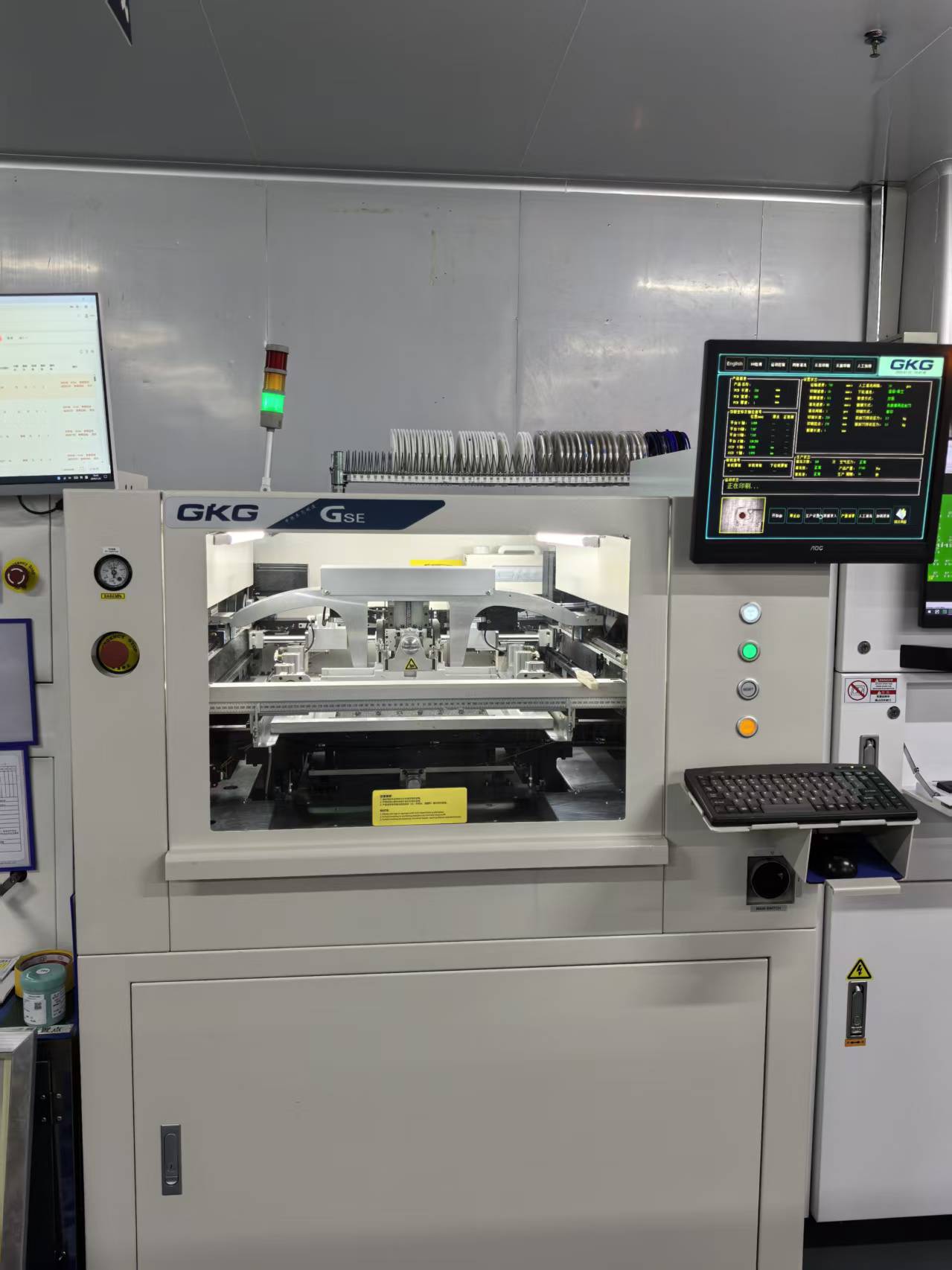
Repositioning accuracy: 0.05±0.025 mm printing precision, defining the ultimate precision benchmark for SMT printing. For micro components such as 0201 chips and high-density ICs with 0.2mm lead pitch, the solder paste forming error is consistently controlled within a tiny margin during printing. Equipped with a top-and-bottom synchronous imaging vision system, it achieves pixel-level alignment even for uneven MARK points. Every printing operation perfectly delivers zero offset and insufficient solder free performance.

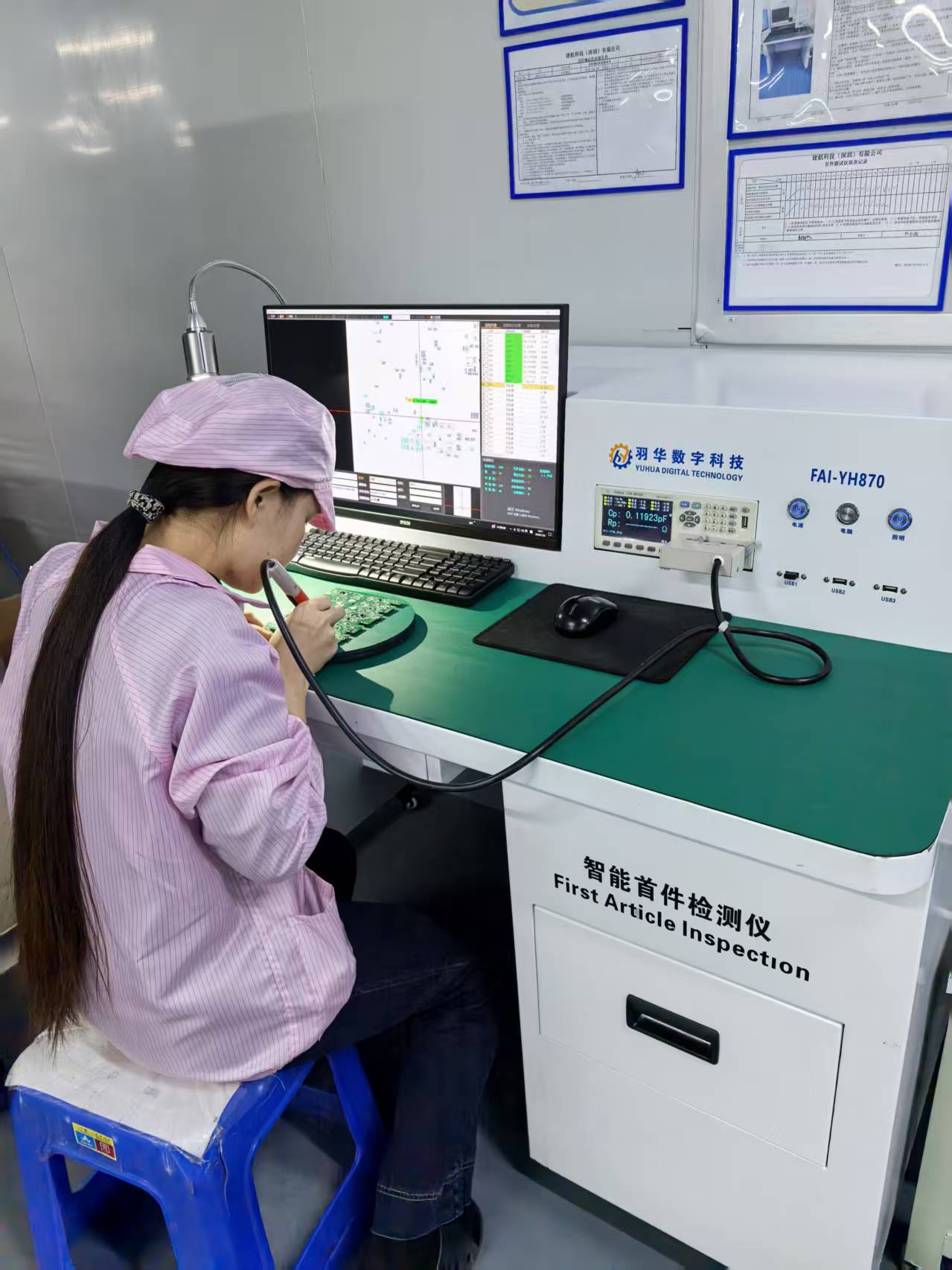
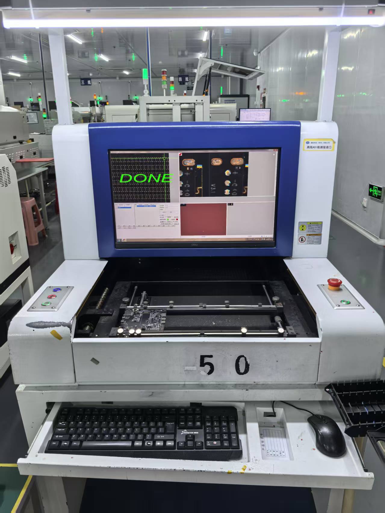
1 Detection Accuracy and Repeatability Core Accuracy: XY positioning accuracy ≤1μm (grating ruler), height measurement accuracy 0.37μm; height repeatability < 1μm (4σ). Minimum Detectable Component: Compatible with 01005 (imperial) / 03015 (metric) micro components, meeting the solder paste inspection requirements for ultra-precision components. Resolution: Standard configuration 13.5μm; optional 10μm, 16.5μm and other specifications, adapting to different requirements of inspection accuracy and speed. 2 Inspection Capability and Efficiency Inspection Items: Capable of detecting volume, area, height, XY offset, shape, etc., and identifying defects such as missing print, excessive solder, insufficient solder, bridging, offset and shape abnormality. Inspection Speed: 0.3–0.35 sec/FOV; Mark recognition speed 0.3–0.5 sec/piece, balancing high speed and high-precision inspection. PCB Substrate & Inspection Range: Standard PCB board size 510×505mm, effective inspection area 480×490mm.

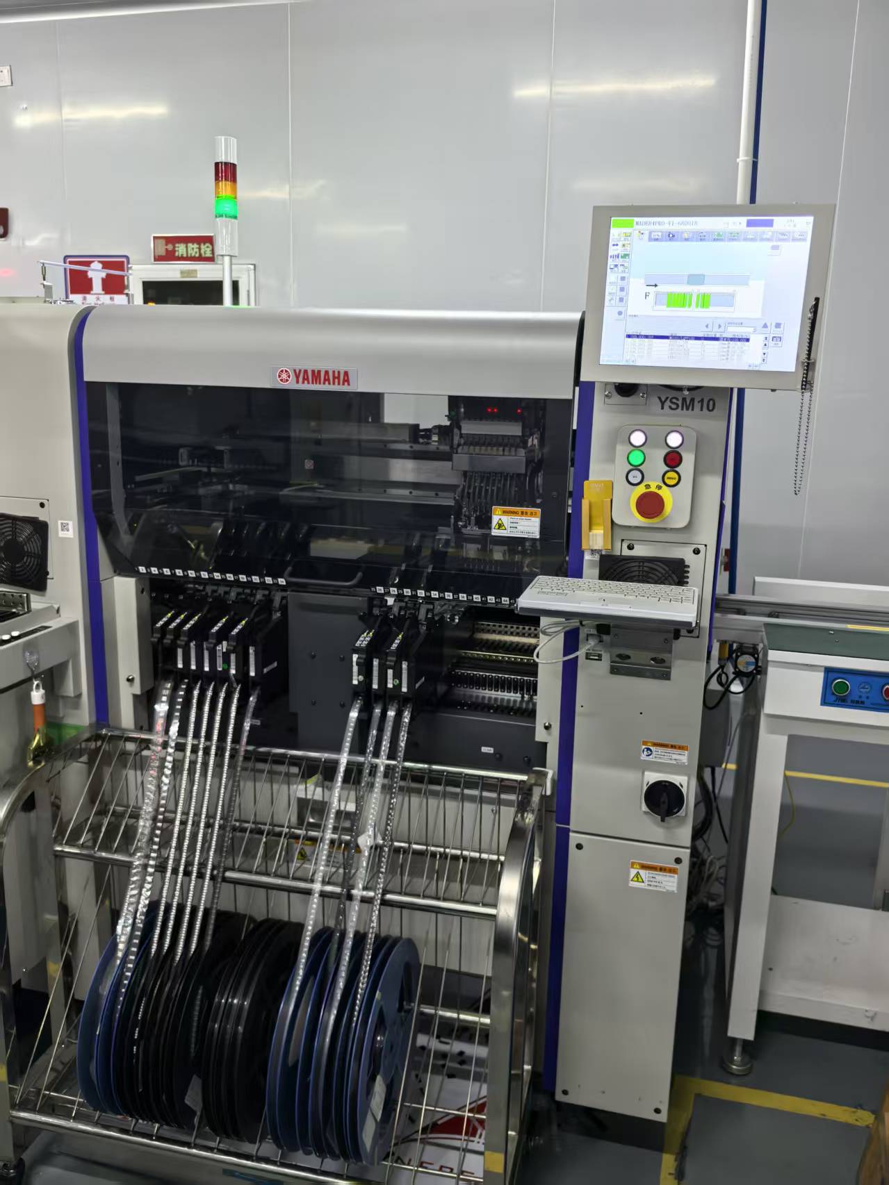
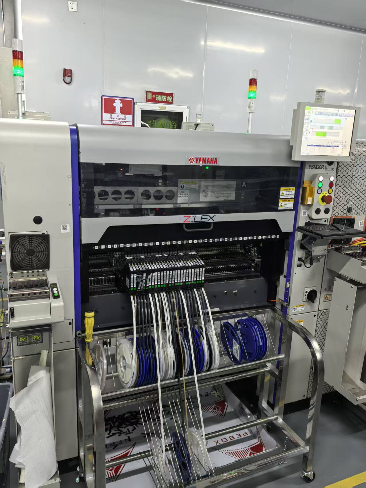
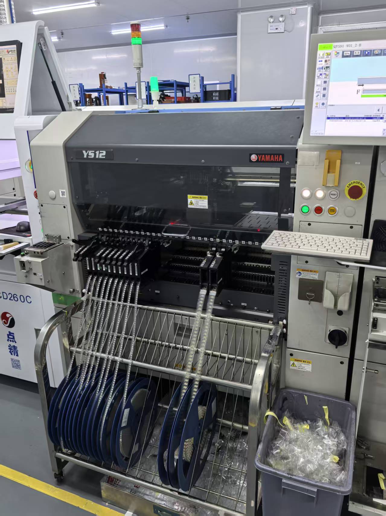
Placement Performance Parameters Placement Capacity: 95,000 CPH; Placement Accuracy: ±0.035mm (±0.025mm), Cpk≥1.0; PCB Board Size (Single Rail): L810×W490mm ~ L50×W50mm; Component Compatibility: Component size range from 0201 up to W55×L100mm.

Placement Performance Parameters Placement Capacity: 95,000 CPH; Placement Accuracy: ±0.035mm (±0.025mm), Cpk≥1.0; PCB Board Size (Single Rail): L810×W490mm ~ L50×W50mm; Component Compatibility: Component size range from 0201 up to W55×L100mm.

Placement Performance Parameters Placement Capacity: HM placement head (10 nozzles) up to 46,000 CPH. Placement Capacity: HM placement head (10 nozzles) approx. 30,000 CPH. Placement Accuracy: For 0201 standard components under optimal conditions: ±0.035 mm (±0.025 mm), Cpk≥1.0. PCB Board Size: Standard applicable range: L510×W460 mm ~ L50×W50 mm. Component Height: ≤15 mm; height over 6.5 mm or size over 12 mm×12 mm.

Repositioning accuracy: 0.05±0.025 mm printing precision, setting the ultimate precision benchmark for SMT printing. For fine pads of 0201 micro-components and high-density ICs with 0.2mm pin pitch, the solder paste printing forming error is always controlled within a microscopic tolerance. Equipped with a top and bottom synchronous imaging vision system, it achieves pixel-level alignment even for uneven MARK points. Every printing process perfectly realizes zero offset and zero insufficient solder.

1 Inspection Accuracy and Repeatability Core Accuracy: XY positioning accuracy ≤ 1 μm (grating scale), height measurement accuracy 0.37 μm; height repeatability < 1 μm (4σ). Minimum Detectable Component: Supports 01005 (imperial) and 03015 (metric) micro components, meeting the solder paste inspection requirements for precision components. Resolution: Standard configuration 13.5 μm; optional specifications including 10 μm, 16.5 μm, to meet different demands for inspection accuracy and speed. 2 Inspection Capacity and Efficiency Inspection Items: Capable of detecting volume, area, height, XY offset, shape and other parameters; identifies defects such as missing printing, excessive solder, insufficient solder, solder bridging, offset and shape defects. Inspection Speed: 0.3–0.35 seconds per FOV; Mark recognition speed 0.3–0.5 seconds per point, balancing high speed and high-precision inspection. PCB Board and Inspection Range: Standard PCB carrier size 510×505 mm, effective inspection area 480×490 mm.

Placement Performance Parameters Placement Capacity: 95,000 CPH; Placement Accuracy: ±0.035 mm (±0.025 mm), Cpk≥1.0; PCB Board Size (Single Rail): L810×W490 mm ~ L50×W50 mm; Component Compatibility: Component size ranging from 0201 up to W55×L100 mm.

Placement Performance Parameters Placement Capacity: 95,000 CPH; Placement Accuracy: ±0.035 mm (±0.025 mm), Cpk≥1.0; PCB Board Size (Single Rail): L810×W490 mm ~ L50×W50 mm; Component Compatibility: Component size ranging from 0201 up to W55×L100 mm.

Placement Performance Parameters Placement Capacity: HM placement head (10 nozzles) up to 46,000 CPH. Placement Capacity: HM placement head (10 nozzles) approximately 30,000 CPH. Placement Accuracy: ±0.035mm (±0.025mm) for 0201 standard components under optimal conditions, Cpk≥1.0. PCB Board Size: Standard applicable range from L510×W460mm down to L50×W50mm. Component Height: ≤15mm; for height over 6.5mm or component size over 12mm×12mm.
Repositioning accuracy: 0.05±0.025 mm printing precision, defining the ultimate precision benchmark for SMT printing. For micro components such as 0201 chips and high-density ICs with 0.2mm lead pitch, the solder paste forming error is consistently controlled within a tiny margin during printing. Equipped with a top-and-bottom synchronous imaging vision system, it achieves pixel-level alignment even for uneven MARK points. Every printing operation perfectly delivers zero offset and insufficient solder free performance.
1 Detection Accuracy and Repeatability Core Accuracy: XY positioning accuracy ≤1μm (grating ruler), height measurement accuracy 0.37μm; height repeatability < 1μm (4σ). Minimum Detectable Component: Compatible with 01005 (imperial) / 03015 (metric) micro components, meeting the solder paste inspection requirements for ultra-precision components. Resolution: Standard configuration 13.5μm; optional 10μm, 16.5μm and other specifications, adapting to different requirements of inspection accuracy and speed. 2 Inspection Capability and Efficiency Inspection Items: Capable of detecting volume, area, height, XY offset, shape, etc., and identifying defects such as missing print, excessive solder, insufficient solder, bridging, offset and shape abnormality. Inspection Speed: 0.3–0.35 sec/FOV; Mark recognition speed 0.3–0.5 sec/piece, balancing high speed and high-precision inspection. PCB Substrate & Inspection Range: Standard PCB board size 510×505mm, effective inspection area 480×490mm.
Placement Performance Parameters Placement Capacity: 95,000 CPH; Placement Accuracy: ±0.035mm (±0.025mm), Cpk≥1.0; PCB Board Size (Single Rail): L810×W490mm ~ L50×W50mm; Component Compatibility: Component size range from 0201 up to W55×L100mm.
Placement Performance Parameters Placement Capacity: 95,000 CPH; Placement Accuracy: ±0.035mm (±0.025mm), Cpk≥1.0; PCB Board Size (Single Rail): L810×W490mm ~ L50×W50mm; Component Compatibility: Component size range from 0201 up to W55×L100mm.
Placement Performance Parameters Placement Capacity: HM placement head (10 nozzles) up to 46,000 CPH. Placement Capacity: HM placement head (10 nozzles) approx. 30,000 CPH. Placement Accuracy: For 0201 standard components under optimal conditions: ±0.035 mm (±0.025 mm), Cpk≥1.0. PCB Board Size: Standard applicable range: L510×W460 mm ~ L50×W50 mm. Component Height: ≤15 mm; height over 6.5 mm or size over 12 mm×12 mm.
Repositioning accuracy: 0.05±0.025 mm printing precision, setting the ultimate precision benchmark for SMT printing. For fine pads of 0201 micro-components and high-density ICs with 0.2mm pin pitch, the solder paste printing forming error is always controlled within a microscopic tolerance. Equipped with a top and bottom synchronous imaging vision system, it achieves pixel-level alignment even for uneven MARK points. Every printing process perfectly realizes zero offset and zero insufficient solder.
1 Inspection Accuracy and Repeatability Core Accuracy: XY positioning accuracy ≤ 1 μm (grating scale), height measurement accuracy 0.37 μm; height repeatability < 1 μm (4σ). Minimum Detectable Component: Supports 01005 (imperial) and 03015 (metric) micro components, meeting the solder paste inspection requirements for precision components. Resolution: Standard configuration 13.5 μm; optional specifications including 10 μm, 16.5 μm, to meet different demands for inspection accuracy and speed. 2 Inspection Capacity and Efficiency Inspection Items: Capable of detecting volume, area, height, XY offset, shape and other parameters; identifies defects such as missing printing, excessive solder, insufficient solder, solder bridging, offset and shape defects. Inspection Speed: 0.3–0.35 seconds per FOV; Mark recognition speed 0.3–0.5 seconds per point, balancing high speed and high-precision inspection. PCB Board and Inspection Range: Standard PCB carrier size 510×505 mm, effective inspection area 480×490 mm.
Placement Performance Parameters Placement Capacity: 95,000 CPH; Placement Accuracy: ±0.035 mm (±0.025 mm), Cpk≥1.0; PCB Board Size (Single Rail): L810×W490 mm ~ L50×W50 mm; Component Compatibility: Component size ranging from 0201 up to W55×L100 mm.
Placement Performance Parameters Placement Capacity: 95,000 CPH; Placement Accuracy: ±0.035 mm (±0.025 mm), Cpk≥1.0; PCB Board Size (Single Rail): L810×W490 mm ~ L50×W50 mm; Component Compatibility: Component size ranging from 0201 up to W55×L100 mm.
Placement Performance Parameters Placement Capacity: HM placement head (10 nozzles) up to 46,000 CPH. Placement Capacity: HM placement head (10 nozzles) approximately 30,000 CPH. Placement Accuracy: ±0.035mm (±0.025mm) for 0201 standard components under optimal conditions, Cpk≥1.0. PCB Board Size: Standard applicable range from L510×W460mm down to L50×W50mm. Component Height: ≤15mm; for height over 6.5mm or component size over 12mm×12mm.
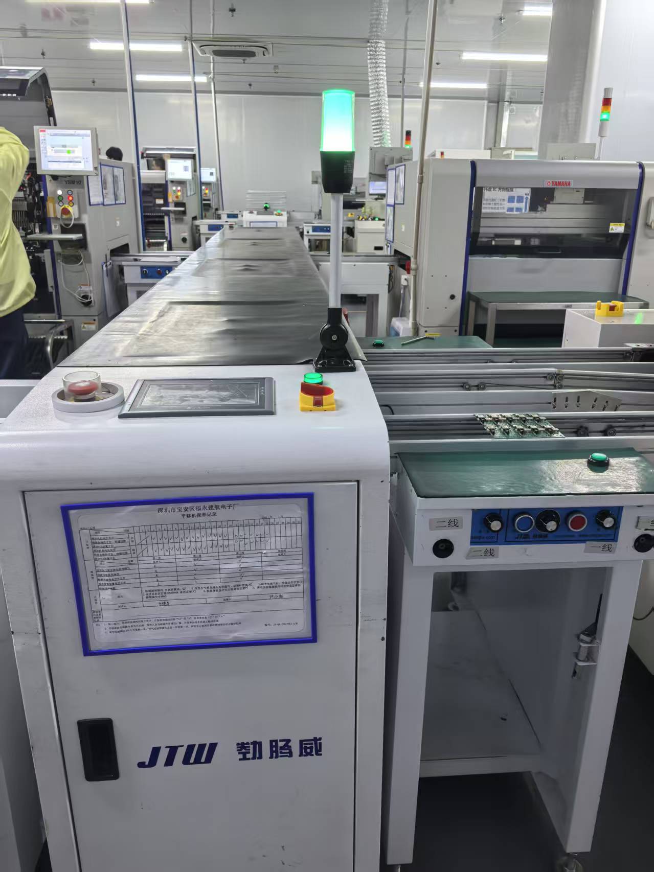
Max Load Capacity: 10 kg per dual rail Rail Mode: Supports 3-in 3-out configuration Working Dimension: 460×510 mm

Temperature Zone Configuration: 13 heating zones with independent upper and lower heating, including preheating, constant temperature, reflow and cooling functional sections. Temperature Control Accuracy: Temperature deviation between set value and actual value ≤ ±1.0℃; temperature fluctuation from no-load to full-load ≤ ±1.5℃. Heating Method: Forced convection heating with efficient thermal compensation, suitable for lead-free and high-precision PCB packaging processes. Conveyor Speed Range: Normal production speed up to 160 cm/min, meeting high-capacity production requirements. Applicable PCB Size: Standard applicable range 50×50mm to 510×460mm; maximum load capacity approx. 3kg. Nitrogen Control: Full-process quantitative nitrogen control; each temperature zone adopts independent closed-loop control. Oxygen concentration can be stably maintained at 50–200ppm (less than 50ppm for semiconductor packaging version). Residual oxygen level supports real-time monitoring, curve recording and traceability. Nitrogen Consumption: Standard closed-loop system with customizable energy-saving mode to effectively reduce nitrogen consumption cost. Flux Recovery: New two-stage flux recovery system.

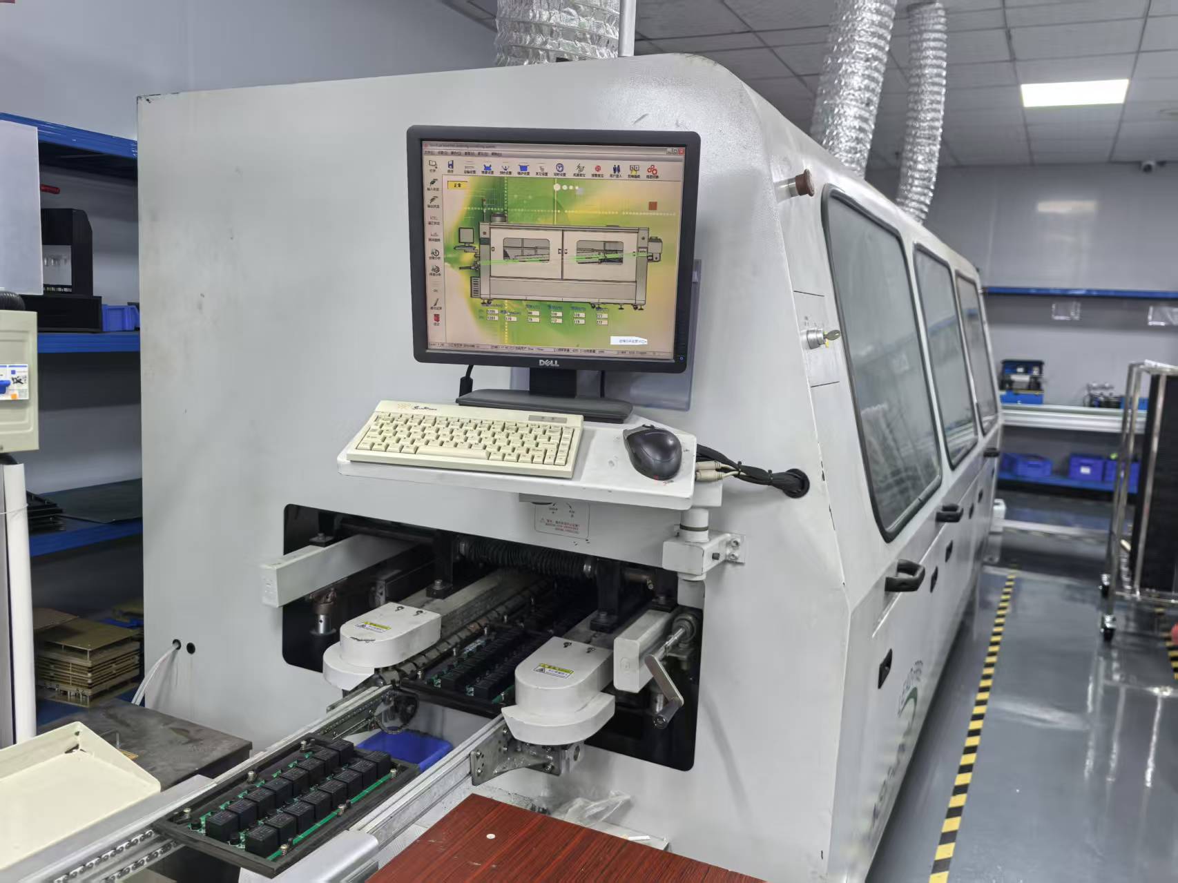
Applicable PCB Size: Standard dual-lane 50×50mm – 530×390mm. PCB Thickness: 0.6–3.0mm, suitable for general SMT production requirements; thick-board model can be customized up to 6.0mm. Conveyor Height: 900±20mm (±30mm for partial models). Conveying Direction: Supports left-to-right / right-to-left bidirectional switching; standard SMEMA interface, compatible with dual-lane production line docking. Conveying Speed: Max 600–1000mm/s, dual lanes with independent drive. Buffer Capacity: Standard 20 layers (layer spacing 25mm).
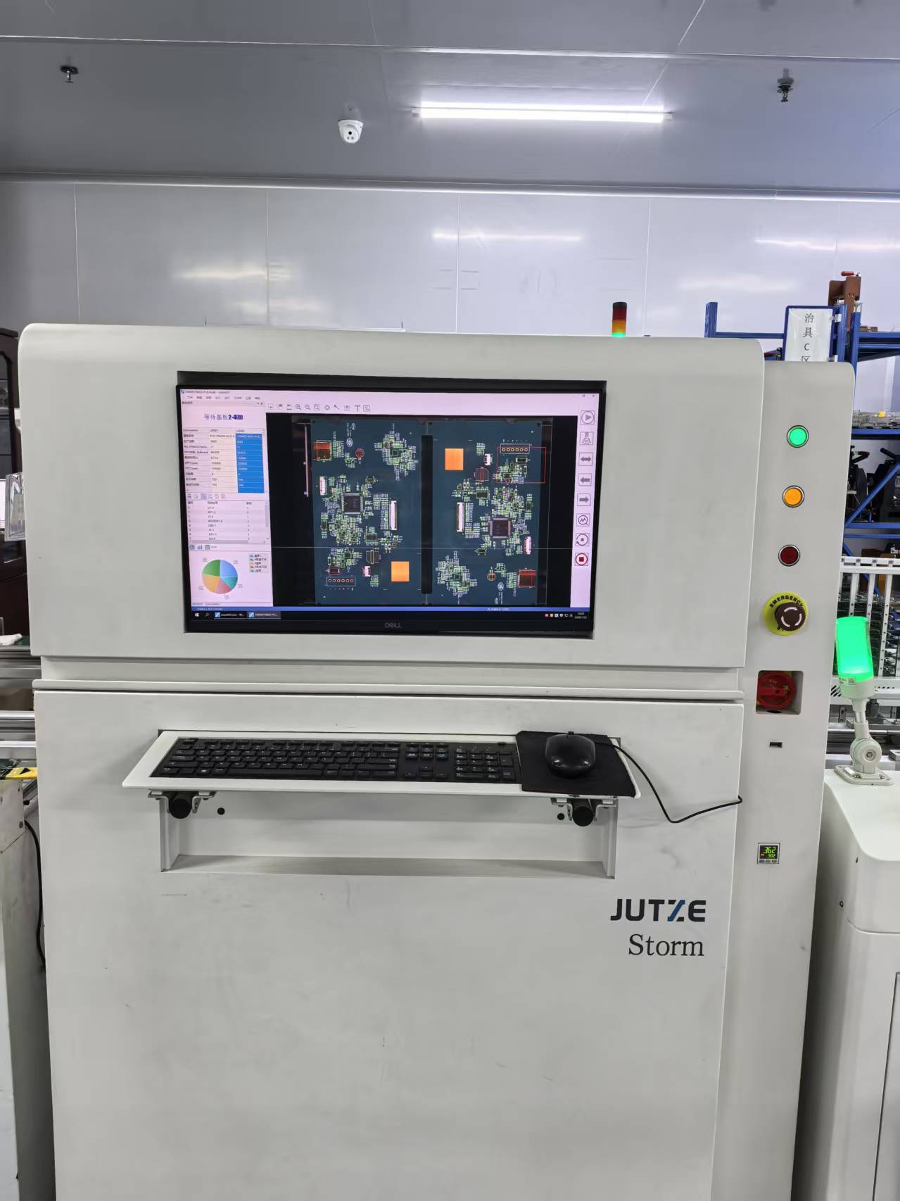
Applicable Size: Dual-lane 50×70mm – 535×330mm. PCB Thickness: 0.6–6.0mm, compatible with standard and thick board production. Minimum Component Inspection: Capable of stable inspection of 0201 (imperial) components with a minimum pin pitch of 0.3mm. Resolution: 5–15μm, meeting the inspection requirements for high-precision packaging and lead-free processes. Imaging System: Equipped with multiple high-resolution industrial CCD cameras, RGB + white light ring light source with time-sharing imaging for clear detail capture. Positioning Accuracy: Grayscale and chromaticity pixel algorithm adopted; positioning accuracy up to 1/16 pixel, ensuring accurate positioning of components and solder joints Defect Coverage: Detects common 2D defects such as missing components, offset, wrong parts, reversed polarity, cold solder joints, bridging, and solder balls.

Repositioning accuracy: 0.05±0.025mm printing precision, setting the ultimate benchmark for SMT printing accuracy. For ultra-fine pads of 0201 micro-components and high-density ICs with 0.2mm pin pitch, the solder paste forming error is kept within minimal tolerances during printing. Equipped with a top-and-bottom synchronous imaging vision system, it achieves pixel-level alignment even on uneven MARK points. Every printing operation delivers precise performance with zero offset and insufficient solder eliminated.
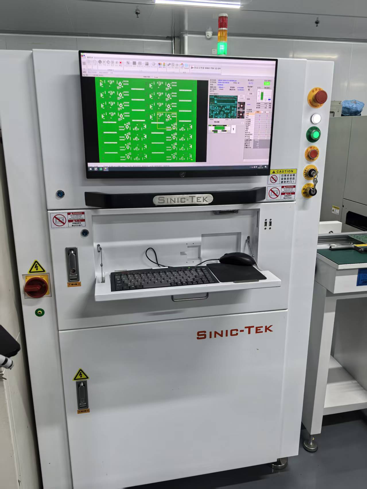
1 Detection Accuracy and Repeatability Core Accuracy: XY positioning accuracy ≤ 1μm (grating ruler), height measurement accuracy 0.37μm; height repeatability accuracy < 1μm (4σ). Minimum Detectable Component: Compatible with ultra-fine components of 01005 (imperial) / 03015 (metric), meeting the solder paste inspection requirements for precision components. Resolution: Standard configuration 13.5μm; optional 10μm, 16.5μm and other specifications to match different demands for inspection accuracy and speed. 2 Inspection Capability and Efficiency Inspection Items: Capable of detecting volume, area, height, XY offset, shape, etc. It can identify defects such as missing print, excessive solder, insufficient solder, solder bridging, offset and shape abnormality. Inspection Speed: 0.3–0.35 seconds per FOV; Mark point recognition speed 0.3–0.5 seconds per point, balancing high speed and precise inspection. PCB Board and Inspection Range: Standard PCB carrier size 510×505mm; effective inspection area 480×490mm.

Mounting Performance Parameters Placement Capacity: 95,000 CPH Placement Accuracy: ±0.035mm (±0.025mm), Cpk ≥ 1.0 PCB Board Size: Single track, L810×W490mm down to L50×W50mm Component Compatibility: Component size from 0201 up to W55×L100mm

Mounting Performance Parameters Placement Capacity: 95,000 CPH Placement Accuracy: ±0.035mm (±0.025mm), Cpk ≥ 1.0 PCB Board Size: Single track, L810×W490mm down to L50×W50mm Component Compatibility: Component size from 0201 up to W55×L100mm
Placement Performance Parameters Placement Capacity: Up to 46,000 CPH with HM placement head (10 nozzles) Placement Capacity: Approximately 30,000 CPH with HM placement head (10 nozzles) Placement Accuracy: For 0201 standard components, ±0.035mm (±0.025mm) under optimal conditions, Cpk ≥ 1.0 PCB Board Size: Standard applicable range from L510×W460mm down to L50×W50mm Component Height: ≤ 15mm; height over 6.5mm or size over 12mm×12mm

Repositioning accuracy: 0.05±0.025 mm printing precision, setting the ultimate benchmark for high-precision SMT printing. For tiny pads of 0201 micro-components and high-density ICs with 0.2 mm pin pitch, solder paste forming errors are consistently controlled within microscopic tolerances. Equipped with a top-and-bottom synchronous imaging vision system, it achieves pixel-level alignment even for uneven MARK points. Every printing operation precisely delivers zero offset and insufficient solder zero defects.

1 Inspection Accuracy & Repeatability Core Accuracy: XY positioning accuracy ≤ 1 μm (grating ruler); height measurement accuracy 0.37 μm; height repeatability < 1 μm (4σ). Minimum Detectable Component: Compatible with ultra-fine components of 01005 (imperial) and 03015 (metric), meeting solder paste inspection requirements for precision components. Resolution: Standard configuration 13.5 μm; optional 10 μm, 16.5 μm and other specifications to adapt to different accuracy and speed requirements. 2 Inspection Capability & Efficiency Inspection Items: Detects volume, area, height, XY offset, shape, etc. Identifies defects such as missing print, excessive solder, insufficient solder, solder bridging, offset and shape abnormality. Inspection Speed: 0.3–0.35 sec/FOV; Mark recognition speed 0.3–0.5 sec/piece, balancing high speed and high precision. PCB & Inspection Range: Standard PCB carrier size 510×505 mm; effective inspection area 480×490 mm.

Placement Performance Parameters Placement Capacity: 95,000 CPH; Placement Accuracy: ±0.035 mm (±0.025 mm), Cpk≥1.0; PCB Board Size (Single Rail): L810×W490 mm ~ L50×W50 mm; Component Compatibility: Component size ranging from 0201 up to W55×L100 mm.

Placement Performance Parameters Placement Capacity: 95,000 CPH; Placement Accuracy: ±0.035 mm (±0.025 mm), Cpk≥1.0; PCB Board Size (Single Rail): L810×W490 mm ~ L50×W50 mm; Component Compatibility: Component size ranging from 0201 up to W55×L100 mm.

Placement Performance Parameters Placement Capacity: HM placement head (10 nozzles) up to 46,000 CPH. Placement Capacity: HM placement head (10 nozzles) approximately 30,000 CPH. Placement Accuracy: ±0.035mm (±0.025mm) for 0201 standard components under optimal conditions, Cpk≥1.0. PCB Board Size: Standard applicable range from L510×W460mm down to L50×W50mm. Component Height: ≤15mm; for height over 6.5mm or component size over 12mm×12mm.

Repositioning accuracy: 0.05±0.025 mm printing precision, defining the ultimate precision benchmark for SMT printing For micro components such as 0201 chips and high-density ICs with 0.2mm lead pitch, the solder paste forming error is consistently controlled within a tiny margin during printing. Equipped with a top-and-bottom synchronous imaging vision system, it achieves pixel-level alignment even for uneven MARK points. Every printing operation perfectly delivers zero offset and insufficient solder free performance.

1 Detection Accuracy and Repeatability Core Accuracy: XY positioning accuracy ≤1μm (grating ruler), height measurement accuracy 0.37μm; height repeatability < 1μm (4σ). Minimum Detectable Component: Compatible with 01005 (imperial) / 03015 (metric) micro components, meeting the solder paste inspection requirements for ultra-precision components. Resolution: Standard configuration 13.5μm; optional 10μm, 16.5μm and other specifications, adapting to different requirements of inspection accuracy and speed. 2 Inspection Capability and Efficiency Inspection Items: Capable of detecting volume, area, height, XY offset, shape, etc., and identifying defects such as missing print, excessive solder, insufficient solder, bridging, offset and shape abnormality. Inspection Speed: 0.3–0.35 sec/FOV; Mark recognition speed 0.3–0.5 sec/piece, balancing high speed and high-precision inspection. PCB Substrate & Inspection Range: Standard PCB board size 510×505mm, effective inspection area 480×490mm.

Placement Performance Parameters Placement Capacity: 95,000 CPH; Placement Accuracy: ±0.035mm (±0.025mm), Cpk≥1.0; PCB Board Size (Single Rail): L810×W490mm ~ L50×W50mm; Component Compatibility: Component size range from 0201 up to W55×L100mm.

Placement Performance Parameters Placement Capacity: 95,000 CPH; Placement Accuracy: ±0.035mm (±0.025mm), Cpk≥1.0; PCB Board Size (Single Rail): L810×W490mm ~ L50×W50mm; Component Compatibility: Component size range from 0201 up to W55×L100mm.

Placement Performance Parameters Placement Capacity: HM placement head (10 nozzles) up to 46,000 CPH. Placement Capacity: HM placement head (10 nozzles) approx. 30,000 CPH. Placement Accuracy: For 0201 standard components under optimal conditions: ±0.035 mm (±0.025 mm), Cpk≥1.0. PCB Board Size: Standard applicable range: L510×W460 mm ~ L50×W50 mm. Component Height: ≤15 mm; height over 6.5 mm or size over 12 mm×12 mm.
Repositioning accuracy: 0.05±0.025 mm printing precision, defining the ultimate precision benchmark for SMT printing. For micro components such as 0201 chips and high-density ICs with 0.2mm lead pitch, the solder paste forming error is consistently controlled within a tiny margin during printing. Equipped with a top-and-bottom synchronous imaging vision system, it achieves pixel-level alignment even for uneven MARK points. Every printing operation perfectly delivers zero offset and insufficient solder free performance.

1 Detection Accuracy and Repeatability Core Accuracy: XY positioning accuracy ≤1μm (grating ruler), height measurement accuracy 0.37μm; height repeatability < 1μm (4σ). Minimum Detectable Component: Compatible with 01005 (imperial) / 03015 (metric) micro components, meeting the solder paste inspection requirements for ultra-precision components. Resolution: Standard configuration 13.5μm; optional 10μm, 16.5μm and other specifications, adapting to different requirements of inspection accuracy and speed. 2 Inspection Capability and Efficiency Inspection Items: Capable of detecting volume, area, height, XY offset, shape, etc., and identifying defects such as missing print, excessive solder, insufficient solder, bridging, offset and shape abnormality. Inspection Speed: 0.3–0.35 sec/FOV; Mark recognition speed 0.3–0.5 sec/piece, balancing high speed and high-precision inspection. PCB Substrate & Inspection Range: Standard PCB board size 510×505mm, effective inspection area 480×490mm.

Placement Performance Parameters Placement Capacity: 95,000 CPH; Placement Accuracy: ±0.035mm (±0.025mm), Cpk≥1.0; PCB Board Size (Single Rail): L810×W490mm ~ L50×W50mm; Component Compatibility: Component size range from 0201 up to W55×L100mm.

Placement Performance Parameters Placement Capacity: 95,000 CPH; Placement Accuracy: ±0.035mm (±0.025mm), Cpk≥1.0; PCB Board Size (Single Rail): L810×W490mm ~ L50×W50mm; Component Compatibility: Component size range from 0201 up to W55×L100mm.

Placement Performance Parameters Placement Capacity: HM placement head (10 nozzles) up to 46,000 CPH. Placement Capacity: HM placement head (10 nozzles) approx. 30,000 CPH. Placement Accuracy: For 0201 standard components under optimal conditions: ±0.035 mm (±0.025 mm), Cpk≥1.0. PCB Board Size: Standard applicable range: L510×W460 mm ~ L50×W50 mm. Component Height: ≤15 mm; height over 6.5 mm or size over 12 mm×12 mm.

Max Load Capacity: 10 kg per dual rail Rail Mode: Supports 3-in 3-out configuration Working Dimension: 460×510 mm

Temperature Zone Configuration: 13 heating zones with independent upper and lower heating, including preheating, constant temperature, reflow and cooling functional sections. Temperature Control Accuracy: Temperature deviation between set value and actual value ≤ ±1.0℃; temperature fluctuation from no-load to full-load ≤ ±1.5℃. Heating Method: Forced convection heating with efficient thermal compensation, suitable for lead-free and high-precision PCB packaging processes. Conveyor Speed Range: Normal production speed up to 160 cm/min, meeting high-capacity production requirements. Applicable PCB Size: Standard applicable range 50×50mm to 510×460mm; maximum load capacity approx. 3kg. Nitrogen Control: Full-process quantitative nitrogen control; each temperature zone adopts independent closed-loop control. Oxygen concentration can be stably maintained at 50–200ppm (less than 50ppm for semiconductor packaging version). Residual oxygen level supports real-time monitoring, curve recording and traceability. Nitrogen Consumption: Standard closed-loop system with customizable energy-saving mode to effectively reduce nitrogen consumption cost. Flux Recovery: New two-stage flux recovery system.

Applicable PCB Size: Standard dual-lane 50×50mm – 530×390mm. PCB Thickness: 0.6–3.0mm, suitable for general SMT production requirements; thick-board model can be customized up to 6.0mm. Conveyor Height: 900±20mm (±30mm for partial models). Conveying Direction: Supports left-to-right / right-to-left bidirectional switching; standard SMEMA interface, compatible with dual-lane production line docking. Conveying Speed: Max 600–1000mm/s, dual lanes with independent drive. Buffer Capacity: Standard 20 layers (layer spacing 25mm).

Applicable Size: Dual-lane 50×70mm – 535×330mm. PCB Thickness: 0.6–6.0mm, compatible with standard and thick board production. Minimum Component Inspection: Capable of stable inspection of 0201 (imperial) components with a minimum pin pitch of 0.3mm. Resolution: 5–15μm, meeting the inspection requirements for high-precision packaging and lead-free processes. Imaging System: Equipped with multiple high-resolution industrial CCD cameras, RGB + white light ring light source with time-sharing imaging for clear detail capture. Positioning Accuracy: Grayscale and chromaticity pixel algorithm adopted; positioning accuracy up to 1/16 pixel, ensuring accurate positioning of components and solder joints. Defect Coverage: Detects common 2D defects such as missing components, offset, wrong parts, reversed polarity, cold solder joints, bridging, and solder balls.

Repositioning accuracy: 0.05±0.025mm printing precision, setting the ultimate benchmark for SMT printing accuracy. For ultra-fine pads of 0201 micro-components and high-density ICs with 0.2mm pin pitch, the solder paste forming error is kept within minimal tolerances during printing. Equipped with a top-and-bottom synchronous imaging vision system, it achieves pixel-level alignment even on uneven MARK points. Every printing operation delivers precise performance with zero offset and insufficient solder eliminated.

1 Detection Accuracy and Repeatability Core Accuracy: XY positioning accuracy ≤ 1μm (grating ruler), height measurement accuracy 0.37μm; height repeatability accuracy < 1μm (4σ). Minimum Detectable Component: Compatible with ultra-fine components of 01005 (imperial) / 03015 (metric), meeting the solder paste inspection requirements for precision components. Resolution: Standard configuration 13.5μm; optional 10μm, 16.5μm and other specifications to match different demands for inspection accuracy and speed. 2 Inspection Capability and Efficiency Inspection Items: Capable of detecting volume, area, height, XY offset, shape, etc. It can identify defects such as missing print, excessive solder, insufficient solder, solder bridging, offset and shape abnormality. Inspection Speed: 0.3–0.35 seconds per FOV; Mark point recognition speed 0.3–0.5 seconds per point, balancing high speed and precise inspection. PCB Board and Inspection Range: Standard PCB carrier size 510×505mm; effective inspection area 480×490mm.

Mounting Performance Parameters Placement Capacity: 95,000 CPH Placement Accuracy: ±0.035mm (±0.025mm), Cpk ≥ 1.0 PCB Board Size: Single track, L810×W490mm down to L50×W50mm Component Compatibility: Component size from 0201 up to W55×L100mm

Mounting Performance Parameters Placement Capacity: 95,000 CPH Placement Accuracy: ±0.035mm (±0.025mm), Cpk ≥ 1.0 PCB Board Size: Single track, L810×W490mm down to L50×W50mm Component Compatibility: Component size from 0201 up to W55×L100mm

Placement Performance Parameters Placement Capacity: Up to 46,000 CPH with HM placement head (10 nozzles) Placement Capacity: Approximately 30,000 CPH with HM placement head (10 nozzles) Placement Accuracy: For 0201 standard components, ±0.035mm (±0.025mm) under optimal conditions, Cpk ≥ 1.0 PCB Board Size: Standard applicable range from L510×W460mm down to L50×W50mm Component Height: ≤ 15mm; height over 6.5mm or size over 12mm×12mm

Repositioning accuracy: 0.05±0.025 mm printing precision, defining the ultimate precision benchmark for SMT printing. For micro components such as 0201 chips and high-density ICs with 0.2mm lead pitch, the solder paste forming error is consistently controlled within a tiny margin during printing. Equipped with a top-and-bottom synchronous imaging vision system, it achieves pixel-level alignment even for uneven MARK points. Every printing operation perfectly delivers zero offset and insufficient solder free performance.

1 Inspection Accuracy & Repeatability Core Accuracy: XY positioning accuracy ≤ 1 μm (grating ruler); height measurement accuracy 0.37 μm; height repeatability < 1 μm (4σ). Minimum Detectable Component: Compatible with ultra-fine components of 01005 (imperial) and 03015 (metric), meeting solder paste inspection requirements for precision components. Resolution: Standard configuration 13.5 μm; optional 10 μm, 16.5 μm and other specifications to adapt to different accuracy and speed requirements. 2 Inspection Capability & Efficiency Inspection Items: Detects volume, area, height, XY offset, shape, etc. Identifies defects such as missing print, excessive solder, insufficient solder, solder bridging, offset and shape abnormality. Inspection Speed: 0.3–0.35 sec/FOV; Mark recognition speed 0.3–0.5 sec/piece, balancing high speed and high precision. PCB & Inspection Range: Standard PCB carrier size 510×505 mm; effective inspection area 480×490 mm.
Placement Performance Parameters Placement Capacity: 95,000 CPH; Placement Accuracy: ±0.035 mm (±0.025 mm), Cpk≥1.0; PCB Board Size (Single Rail): L810×W490 mm ~ L50×W50 mm; Component Compatibility: Component size ranging from 0201 up to W55×L100 mm.

Placement Performance Parameters Placement Capacity: 95,000 CPH; Placement Accuracy: ±0.035 mm (±0.025 mm), Cpk≥1.0; PCB Board Size (Single Rail): L810×W490 mm ~ L50×W50 mm; Component Compatibility: Component size ranging from 0201 up to W55×L100 mm.

Placement Performance Parameters Placement Capacity: HM placement head (10 nozzles) up to 46,000 CPH. Placement Capacity: HM placement head (10 nozzles) approximately 30,000 CPH. Placement Accuracy: ±0.035mm (±0.025mm) for 0201 standard components under optimal conditions, Cpk≥1.0. PCB Board Size: Standard applicable range from L510×W460mm down to L50×W50mm. Component Height: ≤15mm; for height over 6.5mm or component size over 12mm×12mm.

Repositioning accuracy: 0.05±0.025 mm printing precision, setting the ultimate benchmark for high-precision SMT printing. For tiny pads of 0201 micro-components and high-density ICs with 0.2 mm pin pitch, solder paste forming errors are consistently controlled within microscopic tolerances. Equipped with a top-and-bottom synchronous imaging vision system, it achieves pixel-level alignment even for uneven MARK points. Every printing operation precisely delivers zero offset and insufficient solder zero defects.

1 Inspection Accuracy and Repeatability Core Accuracy: XY positioning accuracy ≤ 1 μm (grating scale), height measurement accuracy 0.37 μm; height repeatability < 1 μm (4σ). Minimum Detectable Component: Supports 01005 (imperial) and 03015 (metric) micro components, meeting the solder paste inspection requirements for precision components. Resolution: Standard configuration 13.5 μm; optional specifications including 10 μm, 16.5 μm, to meet different demands for inspection accuracy and speed. 2 Inspection Capacity and Efficiency Inspection Items: Capable of detecting volume, area, height, XY offset, shape and other parameters; identifies defects such as missing printing, excessive solder, insufficient solder, solder bridging, offset and shape defects. Inspection Speed: 0.3–0.35 seconds per FOV; Mark recognition speed 0.3–0.5 seconds per point, balancing high speed and high-precision inspection. PCB Board and Inspection Range: Standard PCB carrier size 510×505 mm, effective inspection area 480×490 mm.

Placement Performance Parameters Placement Capacity: 95,000 CPH; Placement Accuracy: ±0.035mm (±0.025mm), Cpk≥1.0; PCB Board Size (Single Rail): L810×W490mm ~ L50×W50mm; Component Compatibility: Component size range from 0201 up to W55×L100mm.

Placement Performance Parameters Placement Capacity: 95,000 CPH; Placement Accuracy: ±0.035mm (±0.025mm), Cpk≥1.0; PCB Board Size (Single Rail): L810×W490mm ~ L50×W50mm; Component Compatibility: Component size range from 0201 up to W55×L100mm.

Placement Performance Parameters Placement Capacity: HM placement head (10 nozzles) up to 46,000 CPH. Placement Capacity: HM placement head (10 nozzles) approx. 30,000 CPH. Placement Accuracy: For 0201 standard components under optimal conditions: ±0.035 mm (±0.025 mm), Cpk≥1.0. PCB Board Size: Standard applicable range: L510×W460 mm ~ L50×W50 mm. Component Height: ≤15 mm; height over 6.5 mm or size over 12 mm×12 mm.

Repositioning accuracy: 0.05±0.025 mm printing precision, setting the ultimate benchmark for high-precision SMT printing. For tiny pads of 0201 micro-components and high-density ICs with 0.2 mm pin pitch, solder paste forming errors are consistently controlled within microscopic tolerances. Equipped with a top-and-bottom synchronous imaging vision system, it achieves pixel-level alignment even for uneven MARK points. Every printing operation precisely delivers zero offset and insufficient solder zero defects.

1 Inspection Accuracy & Repeatability Core Accuracy: XY positioning accuracy ≤ 1 μm (grating ruler); height measurement accuracy 0.37 μm; height repeatability < 1 μm (4σ). Minimum Detectable Component: Compatible with ultra-fine components of 01005 (imperial) and 03015 (metric), meeting solder paste inspection requirements for precision components. Resolution: Standard configuration 13.5 μm; optional 10 μm, 16.5 μm and other specifications to adapt to different accuracy and speed requirements. 2 Inspection Capability & Efficiency Inspection Items: Detects volume, area, height, XY offset, shape, etc. Identifies defects such as missing print, excessive solder, insufficient solder, solder bridging, offset and shape abnormality. Inspection Speed: 0.3–0.35 sec/FOV; Mark recognition speed 0.3–0.5 sec/piece, balancing high speed and high precision. PCB & Inspection Range: Standard PCB carrier size 510×505 mm; effective inspection area 480×490 mm.

Placement Performance Parameters Placement Capacity: 95,000 CPH; Placement Accuracy: ±0.035 mm (±0.025 mm), Cpk≥1.0; PCB Board Size (Single Rail): L810×W490 mm ~ L50×W50 mm; Component Compatibility: Component size ranging from 0201 up to W55×L100 mm.

Placement Performance Parameters Placement Capacity: 95,000 CPH; Placement Accuracy: ±0.035 mm (±0.025 mm), Cpk≥1.0; PCB Board Size (Single Rail): L810×W490 mm ~ L50×W50 mm; Component Compatibility: Component size ranging from 0201 up to W55×L100 mm.

Placement Performance Parameters Placement Capacity: HM placement head (10 nozzles) up to 46,000 CPH. Placement Capacity: HM placement head (10 nozzles) approximately 30,000 CPH. Placement Accuracy: ±0.035mm (±0.025mm) for 0201 standard components under optimal conditions, Cpk≥1.0. PCB Board Size: Standard applicable range from L510×W460mm down to L50×W50mm. Component Height: ≤15mm; for height over 6.5mm or component size over 12mm×12mm.

Max Load Capacity: 10 kg per dual rail Rail Mode: Supports 3-in 3-out configuration Working Dimension: 460×510 mm
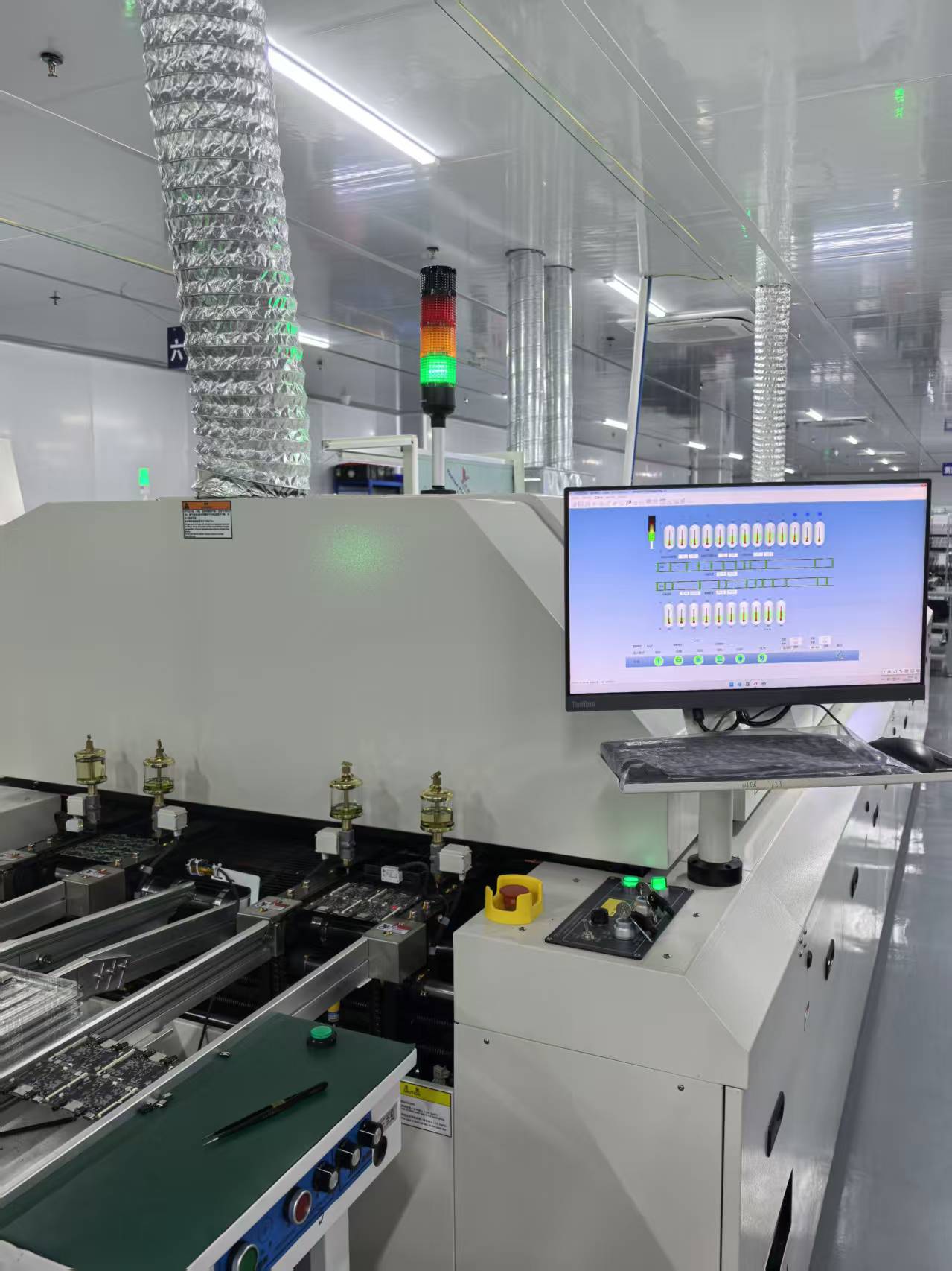
Temperature Zone Configuration: 13 heating zones with independent upper and lower heating, including preheating, constant temperature, reflow and cooling functional sections. Temperature Control Accuracy: Temperature deviation between set value and actual value ≤ ±1.0℃; temperature fluctuation from no-load to full-load ≤ ±1.5℃. Heating Method: Forced convection heating with efficient thermal compensation, suitable for lead-free and high-precision PCB packaging processes. Conveyor Speed Range: Normal production speed up to 160 cm/min, meeting high-capacity production requirements. Applicable PCB Size: Standard applicable range 50×50mm to 510×460mm; maximum load capacity approx. 3kg. Nitrogen Control: Full-process quantitative nitrogen control; each temperature zone adopts independent closed-loop control. Oxygen concentration can be stably maintained at 50–200ppm (less than 50ppm for semiconductor packaging version). Residual oxygen level supports real-time monitoring, curve recording and traceability. Nitrogen Consumption: Standard closed-loop system with customizable energy-saving mode to effectively reduce nitrogen consumption cost. Flux Recovery: New two-stage flux recovery system.
Applicable PCB Size: Standard dual-lane 50×50mm – 530×390mm. PCB Thickness: 0.6–3.0mm, suitable for general SMT production requirements; thick-board model can be customized up to 6.0mm. Conveyor Height: 900±20mm (±30mm for partial models). Conveying Direction: Supports left-to-right / right-to-left bidirectional switching; standard SMEMA interface, compatible with dual-lane production line docking. Conveying Speed: Max 600–1000mm/s, dual lanes with independent drive. Buffer Capacity: Standard 20 layers (layer spacing 25mm).

Applicable Size: Dual-lane 50×70mm – 535×330mm. PCB Thickness: 0.6–6.0mm, compatible with standard and thick board production. Minimum Component Inspection: Capable of stable inspection of 0201 (imperial) components with a minimum pin pitch of 0.3mm. Resolution: 5–15μm, meeting the inspection requirements for high-precision packaging and lead-free processes. Imaging System: Equipped with multiple high-resolution industrial CCD cameras, RGB + white light ring light source with time-sharing imaging for clear detail capture. Positioning Accuracy: Grayscale and chromaticity pixel algorithm adopted; positioning accuracy up to 1/16 pixel, ensuring accurate positioning of components and solder joints. Defect Coverage: Detects common 2D defects such as missing components, offset, wrong parts, reversed polarity, cold solder joints, bridging, and solder balls.

Repositioning accuracy reaches 0.05±0.025 mm in printing precision, setting the benchmark for high-precision SMT printing. For tiny pads of 0201 micro-components and high-density ICs with a 0.2 mm pin pitch, the solder paste forming error is consistently controlled within minimal tolerances. Equipped with a top-and-bottom synchronous imaging vision system, it achieves pixel-level alignment even for uneven MARK points. Every printing operation delivers precise performance with zero offset and insufficient solder.
PCB Size: 50×50mm – 510×460mm, compatible with standard SMT PCB formats. PCB Thickness: 0.5–3.2mm, supporting standard PCB and partial thick-board production. Conveyor Height: 900±20mm, compliant with the standard docking height of SMT production lines. Mounting Efficiency: Up to 36,000 CPH under optimal conditions (0.1 second per CHIP); actual production efficiency ranges from 18,000–25,000 CPH. Mounting Accuracy: Absolute accuracy (μ+3σ) ±0.05mm per CHIP; repeat accuracy (3σ) ±0.03mm per CHIP. Applicable Components: 0201 (metric) up to 32×32mm components; maximum component size 32×32mm, maximum mounting height 6.5mm.
Applicable PCB Size: Standard 50×50mm – 510×460mm. PCB Thickness: 0.6–6.0mm, suitable for standard and thick-board SMT production. Minimum Inspectable Component: Stably inspects 0201 (imperial) and larger components; supports 01005 components. Inspectable Component Types: Covers common SMT components such as resistors, capacitors, inductors, diodes, transistors and ICs; capable of automatically identifying component silkscreen markings and polarity. Testing Accuracy: Equipped with a deeply customized LCR test bridge, achieving a basic measurement accuracy of up to 0.05% for precise and reliable test data. Test Frequency: 20Hz – 300kHz, meeting the LCR parameter testing requirements of various components.
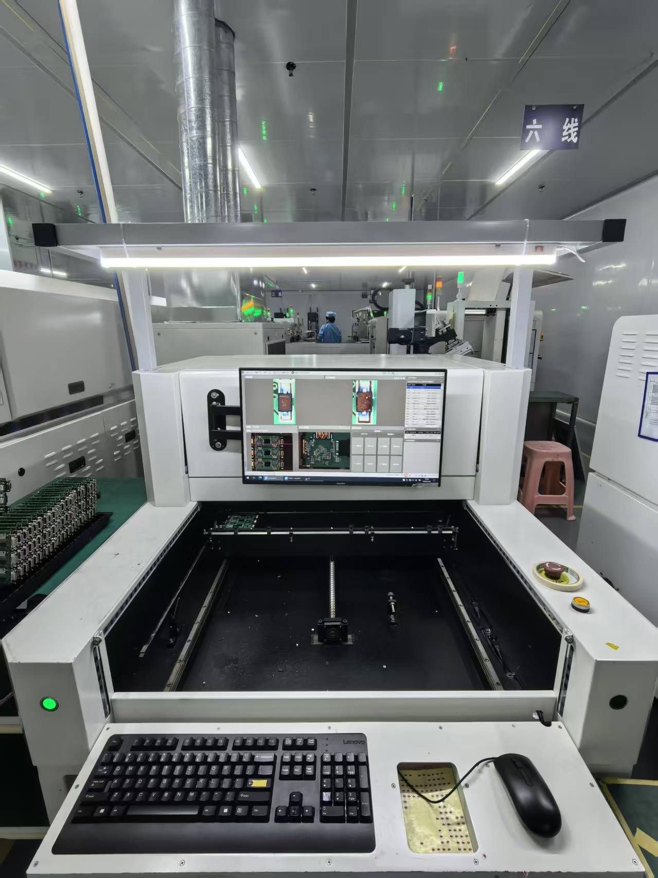
Applicable Size: 50×60mm – 535×330mm PCB Thickness: 0.6–6.0mm, suitable for standard and thick PCB production. Minimum Detectable Component: Stably detects 0201 (imperial) components with a minimum pin pitch of 0.3mm. Resolution: 5–15μm, satisfying inspection requirements for high-precision packaging and lead-free processes. Imaging System: Adopts multiple high-resolution industrial CCD cameras, paired with RGB + white ring light source and time-sharing imaging to capture clear details. Positioning Accuracy: Grayscale and chromaticity pixel algorithm is applied, achieving a positioning accuracy of 1/16 pixel to ensure accurate alignment of components and solder joints. Defect Coverage: Able to detect common 2D defects such as missing components, offset placement, wrong parts, reversed polarity, cold solder joints, bridging, and solder balls.

DIP Irregular Parts Plug-in Assembly
Board Size: 50×50mm – 480×400mm, compatible with standard SMT production board formats. Board Thickness: 0.6–3.0mm, suitable for standard and thick-board SMT production. Conveyor Height: 900±20mm, compliant with standard docking height of SMT production lines. Conveyor Speed: 0.8–2.0m/min, adjustable to meet different soldering process requirements. Conveyor Inclination: 5–7°, adjustable to optimize solder volume and soldering quality.
Applicable Size: 50×60mm – 535×330mm PCB Thickness: 0.6–6.0mm, suitable for standard and thick board production. Resolution: 5–15μm, meeting the inspection requirements of high-precision packaging and lead-free processes. Imaging System: Equipped with multiple high-resolution industrial CCD cameras, adopting RGB + white light ring light source and time-sharing imaging for clear detail capture. Positioning Accuracy: Grayscale and chroma pixel calculation applied; positioning accuracy up to 1/16 pixel, ensuring accurate alignment of components and solder joints. Defect Coverage: Capable of detecting common 2D defects such as missing components, offset parts, wrong components, reversed polarity, cold solder joints, bridging and solder balls.

1.Long component lead trimming after soldering 2.Flux residue cleaning 3.Visual inspection
Automatic Warehousing: Register by scanning codes, automatically allocate storage locations, and trigger early warnings when inventory falls below the set value. Collection & Code Clearance: Adopt FIFO scheduling mode. Solder paste that remains unused within 24 hours after opening will be automatically scrapped; code clearance is required to close the loop after use. Secondary Warehousing: Only allowed in the refrigerated area. Secondary use is restricted if the outbound time or usage times exceed the set limits. Data Reports: Automatically generate operation, temperature and inventory reports, supporting export in Excel and PDF formats. Authority & Traceability: Three-level authority control. Employee ID, time and operation content are automatically recorded. FIFO is supported; the system can connect with MES/ERP, and all data can be exported for traceability.
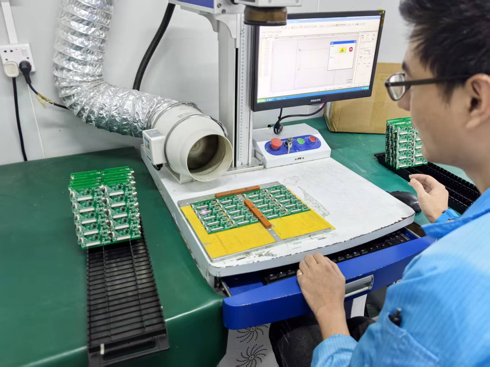
1.Supports laser marking of serial numbers. 2.Supports laser marking of QR codes. 3.Applicable for materials: metal, plastic and wood.
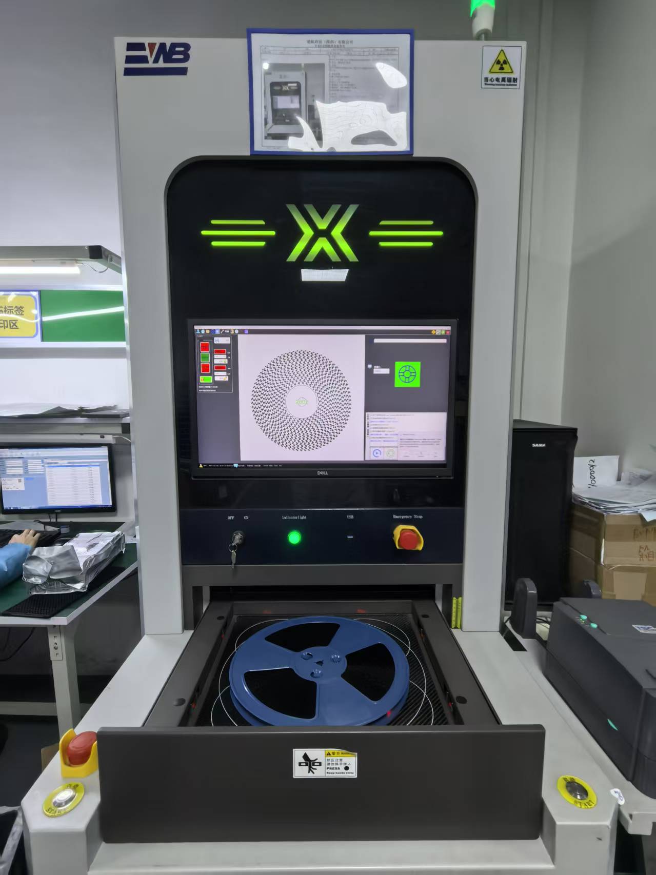
Reel Specifications: Compatible with 7–15 inch reels, supporting reel heights from 5–85 mm; suitable for wafer reels, loose components, moisture-proof vacuum packaging and more. Minimum Component: Able to identify ultra-fine components down to 01005 (imperial) / 0402 (metric), with counting accuracy ≥ 99.99%. Counting Speed: 7–10 seconds per single reel; multi-reel simultaneous counting (e.g., 4 reels) boosts efficiency and matches production line cycle time. Code Scanning Recognition: Supports 1D / 2D codes; minimum readable 1D code 0.13 mm, minimum 2D code 0.25 mm.
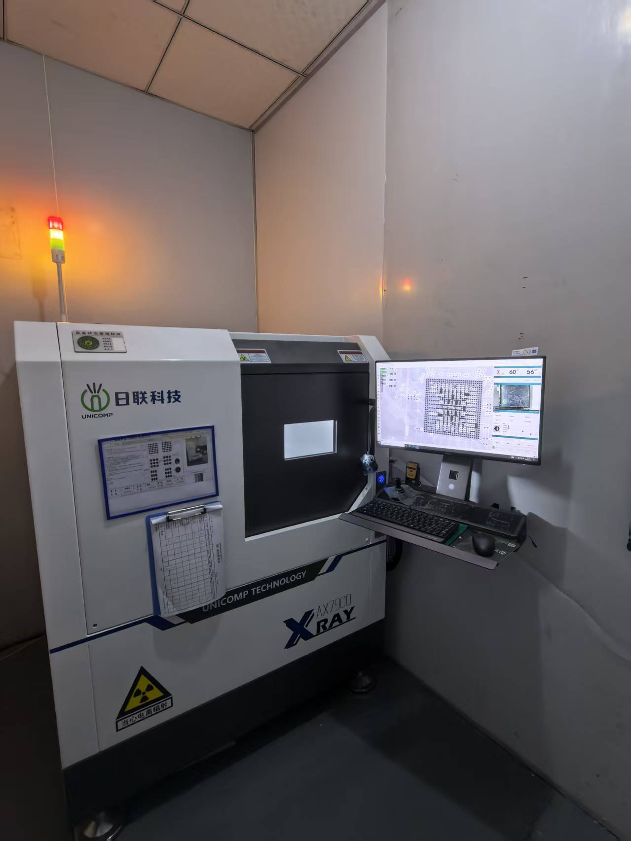
UNIN AX7900 is an offline X-ray inspection system for SMT, BGA and semiconductor applications. Inspection Capability: Automatic BGA void calculation and bubble judgment; optional CNC programming and rotary fixture support. Data Traceability: Inspection results can be exported as Excel reports and connected to MES/ERP systems, with full traceability of operation logs


tel:+86-15766997181
+86-13671491503
E-mail:liuzhen@cmhpcba.com
Address: Room 307, 3rd Floor, Building A, Xinlong Science and Technology Park No. 50 Fengtang Avenue, Fuyong Subdistrict,Bao'an District, Shenzhen City, Guangdong Province, China